


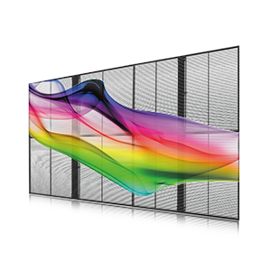


Throughout the development history of the entire LED display, lamp beads have been constantly updated and iterated. Because the LED display is an application-oriented innovation, it is no exaggeration to say that the change of its key device lamp beads leads the changes of the LED display, and the development of the lamp bead leads the development of the LED display. The LED display is full of brilliance, interpreting the colorful world and life. The colorful colors are actually only obtained by superimposing three colors of red, green and blue in different gray scales, so we call red, green and blue the three primary colors of the display industry. Different materials emit different light.
The size of the early light-emitting chip is about 10*13mil. In order to meet the production process requirements of led screen company, the upstream packaging factory will package it. From my entry to the present, there are the following types of packaging in chronological order:
①Dual In-Line Package (DIP)
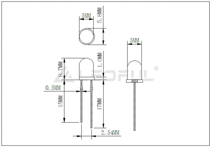
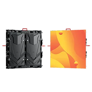
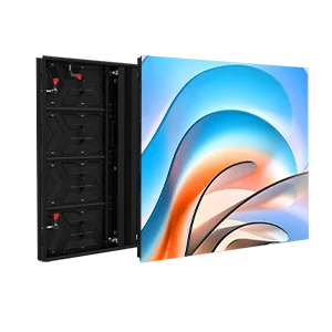
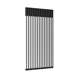
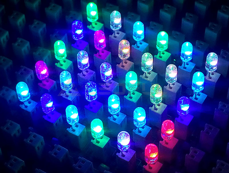
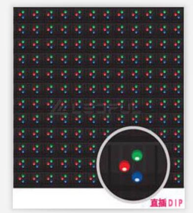
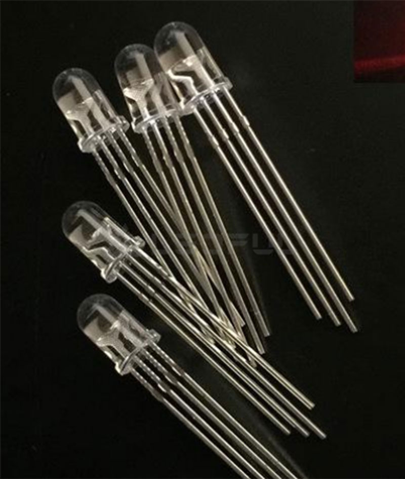
The above picture is a typical dual in-line lamp bead package diagram. The cathode of the LED light-emitting chip is fixed in the reflective cup of the cathode bracket through silver glue (conductive glue), the anode is bound to the anode bracket through gold wire, and then the whole is encapsulated by epoxy resin, thus forming an in-line LED lamp beads. The two brackets are used as the positive and negative poles of the LED lamp bead respectively, and you only need to energize the two poles to light them up. The LED display module made of in-line lamp beads is as shown in the figure below: because the chip used is large, its brightness is high, but its price is expensive and the production efficiency is low, and the red, green and blue chips are separately packaged. The pixels are obviously grainy, and it is impossible to achieve a smaller spacing. Its models have undergone the shrinking iterations of 546, 346, and 246, but the minimum spacing that can be made by 246 is only about P7.62, and the unstable process is difficult, so the models of in-line lamp beads on the market are basically 346.
In order to solve the problems of large volume and low efficiency in the independent packaging of three lamp beads,a few manufacturers have introduced three-in-one packaged in-line lamp beads,Because this kind of lamp bead production equipment is different from conventional dual in-line package, and the production straight-through rate is not high, only a few manufacturers in the industry are currently using it.
②Surface Mounted Device(SMD)
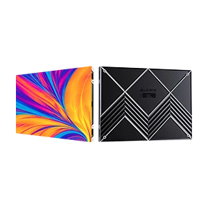
As the spacing of LED displays continues to become smaller, SMD lamp beads have begun to be widely used, which are divided into two categories: TOP type and CHIP type.
1.TOP type
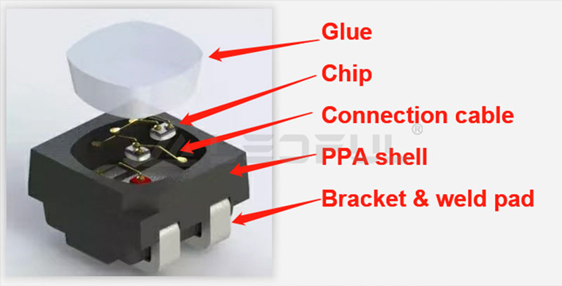
The TOP type is also called the bracket type. It encapsulates three light-emitting chips of red, green and blue at the same time. As shown in the figure, one electrode of the red light chip is fixed by conductive glue and connected to the bracket, and the other electrode is connected to the bracket by gold wire. The blue-green light chip is fixed on the support of the red light chip by conductive glue, and the two electrodes are respectively bound and connected to the support by gold wires. (If the bracket on which the chip is placed is the positive pole of the chip, we call it a common anode lamp bead, otherwise it is a common cathode lamp bead). The PPA shell is sealed and forms a reflector, which is filled with clear glue (usually epoxy) to allow light to escape. The brackets are bent at the bottom to form the SMD pads.
2. CHIP type
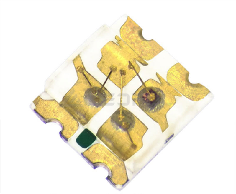
The size of the TOP type is limited by the bracket. When the lamp bead becomes small to a certain extent, it can only use the CHIP type package. At present, the 1010 is a dividing line, the CHIP type below 1010, the TOP type above 1010, and the 1010 has both TOP and CHIP. As shown in the picture above, the bottom is a PCB substrate, the bracket in the TOP type becomes a PCB circuit in the CHIP type,The bottom pad is formed through the semi-circular hole on the edge of the PCB substrate. The chip fixing method will not be described in detail. The upper end of the chip is molded with a layer of glue (usually epoxy resin).